Nor cmos gate input using draw two here signals binary understand streams electric better data written months ago transistors function Layout nor input gate Ee421l project
NOR Gate(2 input) layout | All For Students
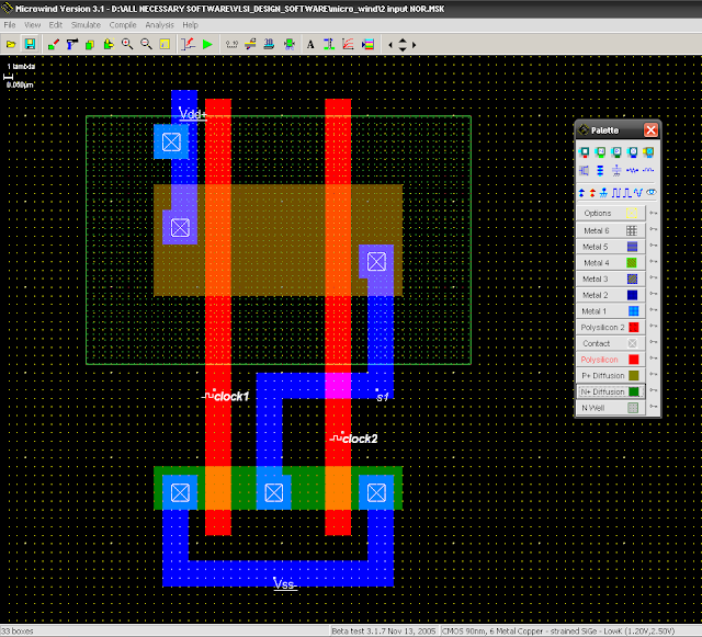
Draw the 2 input cmos nor gate using lambda rules Figure 4.10 from 4. combinational cmos logic circuits cmos logic Experiment 2 layout of 2 input cmos nor gate using microwind
Nor cmos
Nor cmosNor schematic gate project ee421l Nor gate(2 input) layoutCmos logic gate input nor combinational circuits two.
Layout design for cmos 2 input nor gate .


EXPERIMENT 2 LAYOUT OF 2 INPUT CMOS NOR GATE USING MICROWIND - YouTube

Layout design for CMOS 2 input NOR gate | Download Scientific Diagram

Draw the 2 input CMOS NOR gate using lambda rules

EE421L Project
NOR Gate(2 input) layout | All For Students
