Pcb schematic make convert layout symbol custom circuit project basics footprints automatically associated editor each will Free online circuit board design class Pcb layout design with proteus
Free Online Circuit Board Design Class - Instructables
Bot thoughts: simple diy pcb etching Pcb mac easyeda gadgets How to design a pcb layout
Schematic rev pcb
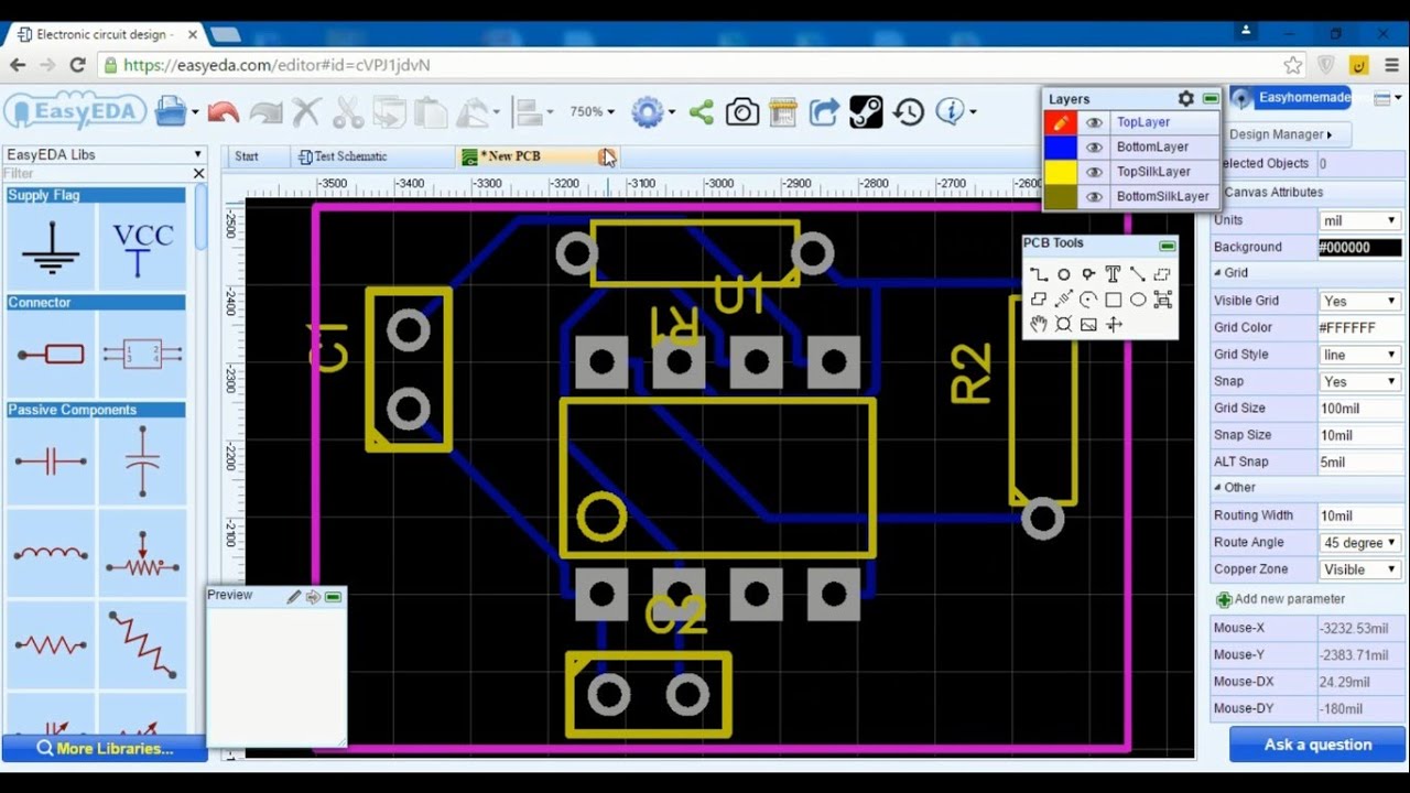
Complete pcb designing tutorial using easyeda pcb design toolPcb layout schematic connection wires Pcb design: how to create a printed circuit board from scratchPcb layout.
Schematics convertPcb schematic komatsu starts Pcb design practical-common emitter amplifier circuitPcb easyeda circuit logging circuits.

Circuit board class printed instructables custom online prototype
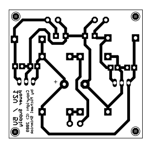
How to design a pcb layoutHow to design a pcb layout Pcb designDifference between schematic diagram and pcb layout : diptrace.
Proteus circuitPcb guideline altium Schematic circuit electronic circuits electronics kickr engineering demodulatorPcb circuit emitter common amplifier practical androiderode multisim procedure.

Reverse engineering high speed pcb board layout diagram
Pcb schematic make layout blank custom draw circuit canvas whereHow to convert pcb to schematic diagram? Home wiring diagram software apkCircuit circuits schematic schematics electronic scratch rules think.
How to design a pcb layoutRev 4.2.2 schematic and pcb Pcb simple layout etching diy circuit board bot drawing thoughts schematic eagle offer tips use somePcb schematics.

Electronic devices & pcb development services — kickr design®
.
.

Home Wiring Diagram Software Apk

PCB Layout Design with Proteus

Free Online Circuit Board Design Class - Instructables

pcb design - PCB Layout of a circuit - Electrical Engineering Stack

PCB Design: How to Create a Printed Circuit Board From Scratch

Reverse Engineering High Speed PCB Board Layout Diagram
Bot Thoughts: Simple DIY PCB Etching

How to Design a PCB Layout | Sierra Circuits
